Kicad 7 How To Move From Schematic To Pcb Design A Pcb For T
Micky's fab academy Kicad pcb layout Kicad – pcb layout – basicpi
Micky's Fab Academy
Design a pcb for the very first time in kicad : 9 steps (with pictures Download free kicad 7 schematic capture pcb layout Kicad pcb route circuit
Kicad generate pcb from schematic
Design a pcb for the very first time in kicad : 9 steps (with picturesCreating a pcb in everything: kicad, part 1 Download free kicad 7 schematic capture pcb layoutTop 10 best and free pcb layout design software in 2023.
Kicad pcb schematic component footprints assign select tools menu firstHow to create your first kicad pcb project? How to create your first kicad pcb project?How to create your first kicad pcb project?.

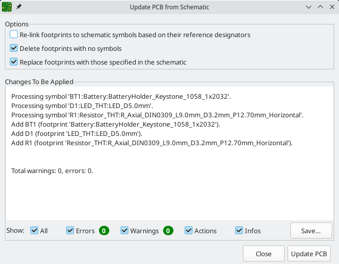
Step-by-step on introduction to kicad
Kicad pcb schematicsKicad pcb hackaday nanite wesley Pcb kicad daumemoHow to convert schematic to pcb layout in kicad.
Kicad create pcb from schematicSchematic to pcb in kicad Pcb design: laying out the board in kicadHow do i convert a schematic to pcb layout in kicad (step by step).

Make this into kicad, and provide schematic and pcb
Kicad pcb schematic creating everything part hackaday completed board ourKicad schematic wires connecting components circuits Comenzando en kicadHow to route a pcb in kicad.
Design a pcb for the very first time in kicad : 9 steps (with picturesHow do i convert a schematic to pcb layout in kicad ? – pcb hero Kicad 7 pcb layout in 5 stepsKicad pcb daumemo.

Kicad pcb daumemo
Creating a pcb in everything: kicad, part 2Solved i need help turning this circuit into kicad pcb, i Pcb designing part 1: how to design the schematics (kicad)Kicad tutorial: make your first printed circuit board.
Kicad pcb laying speculatrix#10 how to do pcb routing in kicad 7.0 with basic pcb design rules Download free kicad 7 schematic capture pcb layoutDesign a pcb for the very first time in kicad : 9 steps (with pictures.


Make this into KICAD, and provide schematic and PCB | Chegg.com

How to create your first KiCAD PCB project? - Daumemo

Download Free Kicad 7 Schematic Capture PCB Layout - Xtronic
Comenzando en KiCad | 7.0 | Español | Documentation | KiCad

Design a PCB for the Very First Time in KiCad : 9 Steps (with Pictures

KiCad Tutorial: Make Your First Printed Circuit Board

#10 How To Do PCB Routing In KiCad 7.0 with Basic PCB Design Rules | #

Design a PCB for the Very First Time in KiCad : 9 Steps (with Pictures